Modern electronic products demand higher speed, improved reliability, lower power consumption, and compact designs. Whether you’re developing an industrial automation controller, IoT device, medical equipment, automotive electronics, or an embedded system, the quality of your Printed Circuit Board (PCB) design directly impacts the overall performance of the product.
A well-designed PCB minimizes electrical noise, improves signal integrity, enhances thermal performance, and ensures long-term reliability. In this article, we explore the best PCB design practices that help engineers develop high-performance electronic products.
Why PCB Design Matters
A PCB is much more than a platform for mounting electronic components. It determines how efficiently signals travel, how heat is dissipated, and how reliably the system operates under different environmental conditions.
Poor PCB design can lead to:
- Signal interference and EMI issues
- Excessive heat generation
- Voltage drops
- Random system failures
- Manufacturing defects
- Reduced product lifespan
Following proven PCB design practices significantly reduces development time and improves product quality.
1. Start with a Proper PCB Stack-Up
The PCB stack-up defines the arrangement of copper and dielectric layers.
A proper stack-up helps:
- Maintain controlled impedance
- Reduce electromagnetic interference (EMI)
- Improve signal integrity
- Simplify routing
For high-speed electronics, multilayer PCBs with dedicated power and ground planes provide superior performance compared to two-layer boards.
2. Plan Component Placement Carefully
Component placement is one of the most critical stages in PCB design.
Best practices include:
- Place related components close together.
- Keep signal paths short.
- Position decoupling capacitors near IC power pins.
- Separate analog and digital circuits.
- Keep high-current components away from sensitive signals.
- Place connectors logically for easy assembly.
Good placement often eliminates routing problems before they occur.
3. Maintain Proper Grounding
A continuous ground plane is essential for high-performance electronics.
Benefits include:
- Lower electrical noise
- Better return current paths
- Reduced EMI
- Improved signal quality
Avoid splitting the ground plane unless absolutely necessary. A solid ground reference improves overall PCB performance.
4. Optimize Power Distribution
Stable power delivery is crucial for reliable operation.
Recommendations:
- Use wider traces for power lines.
- Add multiple decoupling capacitors.
- Keep power loops small.
- Use dedicated power planes for high-current applications.
- Minimise voltage drops across long traces.
Proper power integrity reduces unexpected system resets and improves overall stability.
5. Follow High-Speed Routing Rules
As operating frequencies increase, PCB traces behave like transmission lines.
High-speed routing practices include:
- Match differential pair lengths.
- Maintain controlled impedance.
- Avoid unnecessary vias.
- Keep clock signals short.
- Route critical signals first.
- Minimize sharp 90° bends.
These techniques preserve signal quality and reduce timing errors.
6. Reduce Electromagnetic Interference (EMI)
EMI can affect both your product and nearby electronic equipment.
To minimize EMI:
- Keep high-speed traces short.
- Use ground stitching vias.
- Separate noisy and sensitive circuits.
- Minimize current loop areas.
- Add proper shielding when required.
- Use EMI filters on external interfaces.
Meeting EMC standards becomes much easier with proper PCB layout.
7. Design for Thermal Management
Heat is one of the biggest enemies of electronic components.
Thermal management techniques include:
- Use thermal vias.
- Increase copper area.
- Add heat sinks where necessary.
- Keep heat-generating components apart.
- Optimize airflow around power devices.
Lower operating temperatures increase component lifespan and reliability.
8. Select the Right Trace Width
Trace width depends on:
- Current carrying capacity
- Temperature rise
- Copper thickness
- Manufacturing capability
Undersized traces may overheat, while oversized traces consume unnecessary board space. Use PCB trace width calculators during design.
9. Keep Design for Manufacturability (DFM) in Mind
A design that works electrically but cannot be manufactured efficiently increases production costs.
DFM recommendations:
- Maintain adequate component spacing.
- Use standard hole sizes.
- Follow PCB manufacturer design rules.
- Avoid unnecessary complexity.
- Ensure sufficient solder mask clearance.
- Provide fiducial marks for automated assembly.
Manufacturing-friendly designs reduce defects and improve production yield.
10. Design for Testability (DFT)
Testing should never be an afterthought.
Include:
- Accessible test points
- Programming headers
- Boundary scan support (where applicable)
- Clearly labeled connectors
- Easy probe access
DFT simplifies production testing and field maintenance.
11. Verify with Design Rule Checks (DRC)
Before manufacturing, perform comprehensive verification.
Checklist:
- Electrical Rule Check (ERC)
- Design Rule Check (DRC)
- Signal Integrity Analysis
- Power Integrity Analysis
- Thermal Analysis
- 3D Mechanical Verification
Early verification prevents expensive PCB revisions.
12. Choose Quality Components
Even the best PCB layout cannot compensate for poor-quality components.
When selecting components:
- Verify availability
- Consider lifecycle status
- Check temperature ratings
- Ensure voltage margins
- Use trusted manufacturers
Reliable components improve product longevity and reduce maintenance costs.
Common PCB Design Mistakes to Avoid
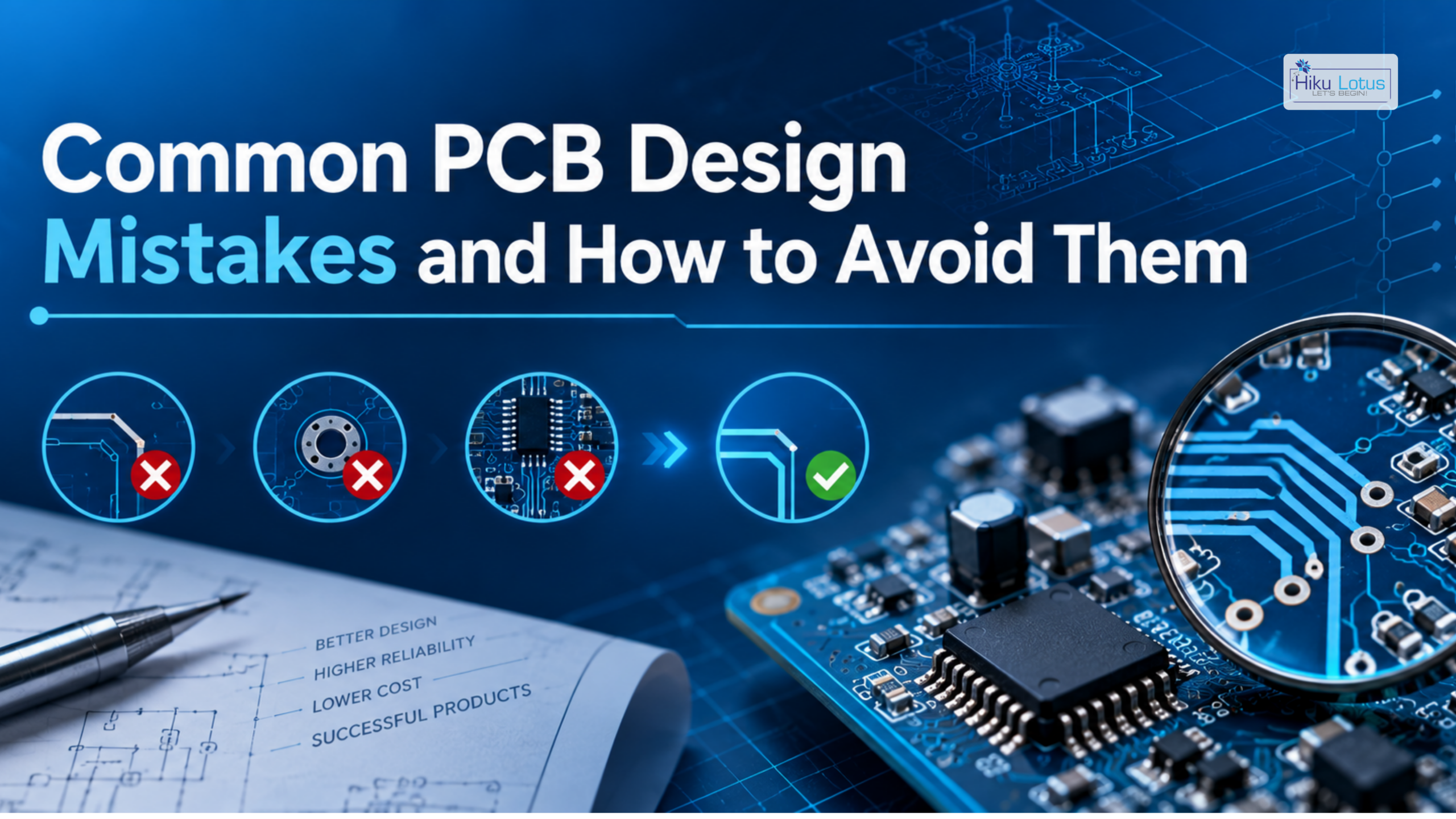
Many PCB failures result from avoidable design errors, including:
- Poor grounding
- Long signal loops
- Inadequate decoupling
- Incorrect footprint dimensions
- Overcrowded layouts
- Excessive vias
- Poor thermal design
- Ignoring manufacturer guidelines
Avoiding these mistakes saves time, cost, and multiple design revisions.
Industries That Benefit from High-Quality PCB Design
Professional PCB design plays a vital role across various industries, including:
- Industrial Automation
- Consumer Electronics
- Medical Devices
- Automotive Electronics
- IoT Products
- Robotics
- Telecommunications
- Aerospace & Defense
- Gaming & Amusement Systems
- Smart Control Systems
Each application has unique performance, reliability, and compliance requirements that demand expert PCB engineering.
Why Choose Hiku Lotus for PCB Design Services?
At Hiku Lotus, we specialize in designing high-performance, reliable, and manufacturing-ready PCBs tailored to your application. Our engineering team combines industry experience with modern design tools to deliver solutions that meet performance, quality, and production requirements.
Our PCB design capabilities include:
- Custom PCB Design
- Multi-Layer PCB Layout
- High-Speed PCB Design
- Embedded System Hardware Design
- Schematic Capture
- PCB Reverse Engineering
- Design Optimization
- Prototype Development
- Design Verification
- DFM & DFT Review
- Electronics Product Development
Whether you’re developing a new product or improving an existing design, Hiku Lotus delivers PCB solutions that help accelerate innovation while ensuring reliability and scalability.
Conclusion
A high-performance electronic product begins with a well-designed PCB. From component placement and grounding to thermal management and manufacturability, every design decision influences the final product’s reliability and efficiency.
By following industry best practices, engineers can reduce development risks, improve product quality, and achieve faster time-to-market.
If you’re looking for professional PCB design services, Hiku Lotus offers end-to-end electronics design solutions—from concept and schematic design to PCB layout, prototyping, and production support.
Talk to Hiku Lotus About Your PCB Design Project
From schematic design and PCB layout to prototype development and production support, Hiku Lotus delivers high-performance PCB solutions tailored to your product requirements. Get in touch with our team to discuss your next electronics project.
Frequently Asked Questions (FAQs)
What is the most important factor in PCB design?
Proper component placement, grounding, power distribution, and signal routing are the foundation of a reliable PCB design.
Why is a multilayer PCB preferred for high-performance electronics?
Multilayer PCBs provide dedicated power and ground planes, better signal integrity, lower EMI, and improved thermal performance.
How can EMI be reduced in PCB design?
EMI can be minimized through proper grounding, shorter trace lengths, controlled impedance routing, shielding, and optimized component placement.
What is Design for Manufacturability (DFM)?
DFM ensures that a PCB can be manufactured efficiently, reducing production costs, assembly issues, and defects.
Does Hiku Lotus provide custom PCB design services?
Yes. Hiku Lotus provides custom PCB design, schematic development, multilayer PCB layout, embedded hardware design, prototyping, testing, and production support for industrial and commercial applications.