Every successful electronic product starts with an idea.
It may begin as a simple concept, a hand-drawn circuit, a functional requirement, an existing product that needs improvement, or a prototype that needs to be converted into a reliable PCB. Turning that idea into a working electronic product requires much more than simply designing a circuit board.
A successful electronics development process combines requirements analysis, circuit design, component selection, PCB design, embedded systems, firmware development, prototyping, testing, debugging, and manufacturing considerations.
At Hiku Lotus, we help businesses transform electronics concepts into practical, reliable, and production-ready solutions. From the initial idea to PCB development and prototype testing, our engineering approach focuses on building products that meet functional, electrical, mechanical, and commercial requirements.
Why a Structured Electronics Development Process Matters
Electronics development involves many interconnected decisions.
A small change in the power supply can affect component selection. A change in the enclosure can affect PCB dimensions. A high-speed communication interface can influence the PCB stack-up and routing strategy. Similarly, firmware requirements can influence the choice of microcontroller.
Without a structured development process, these dependencies can lead to:
- Design changes
- Prototype failures
- Higher development costs
- Component availability problems
- PCB redesigns
- Manufacturing difficulties
- Performance issues
- Delayed product launches
A systematic approach helps identify potential problems early and reduces unnecessary iterations.
Our Electronics Development Process
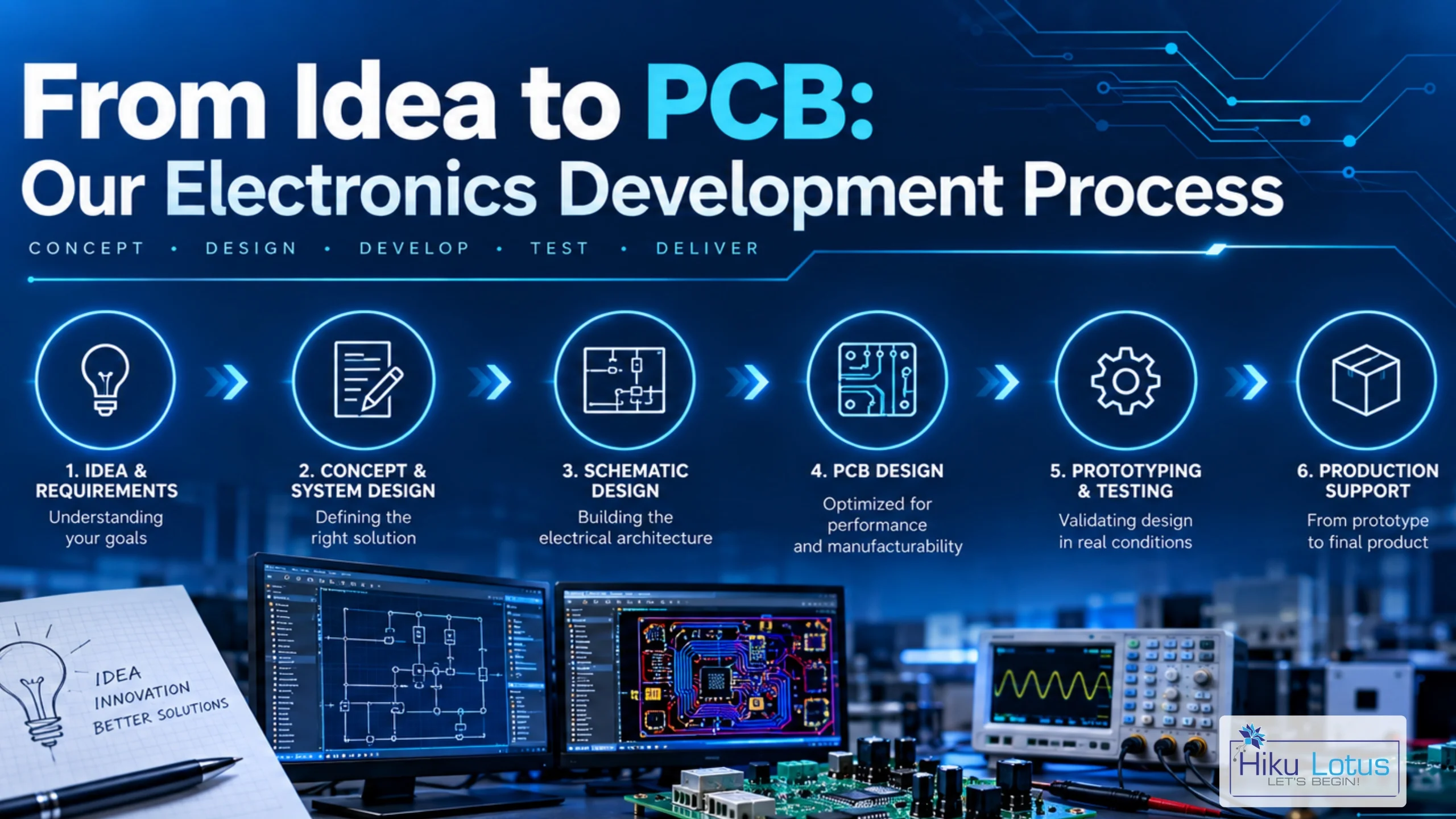
A typical electronics development journey at Hiku Lotus can be divided into several key stages:
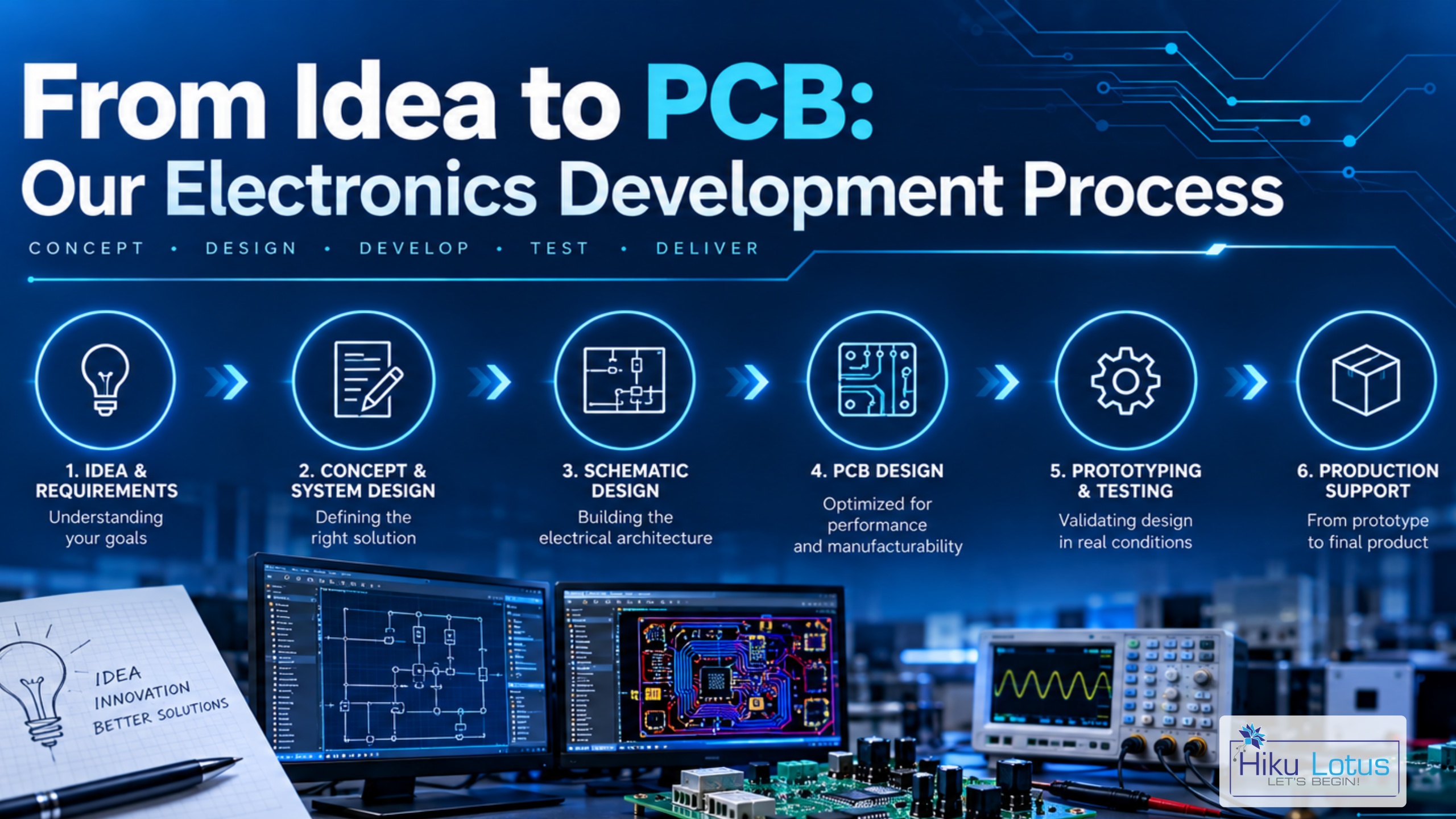
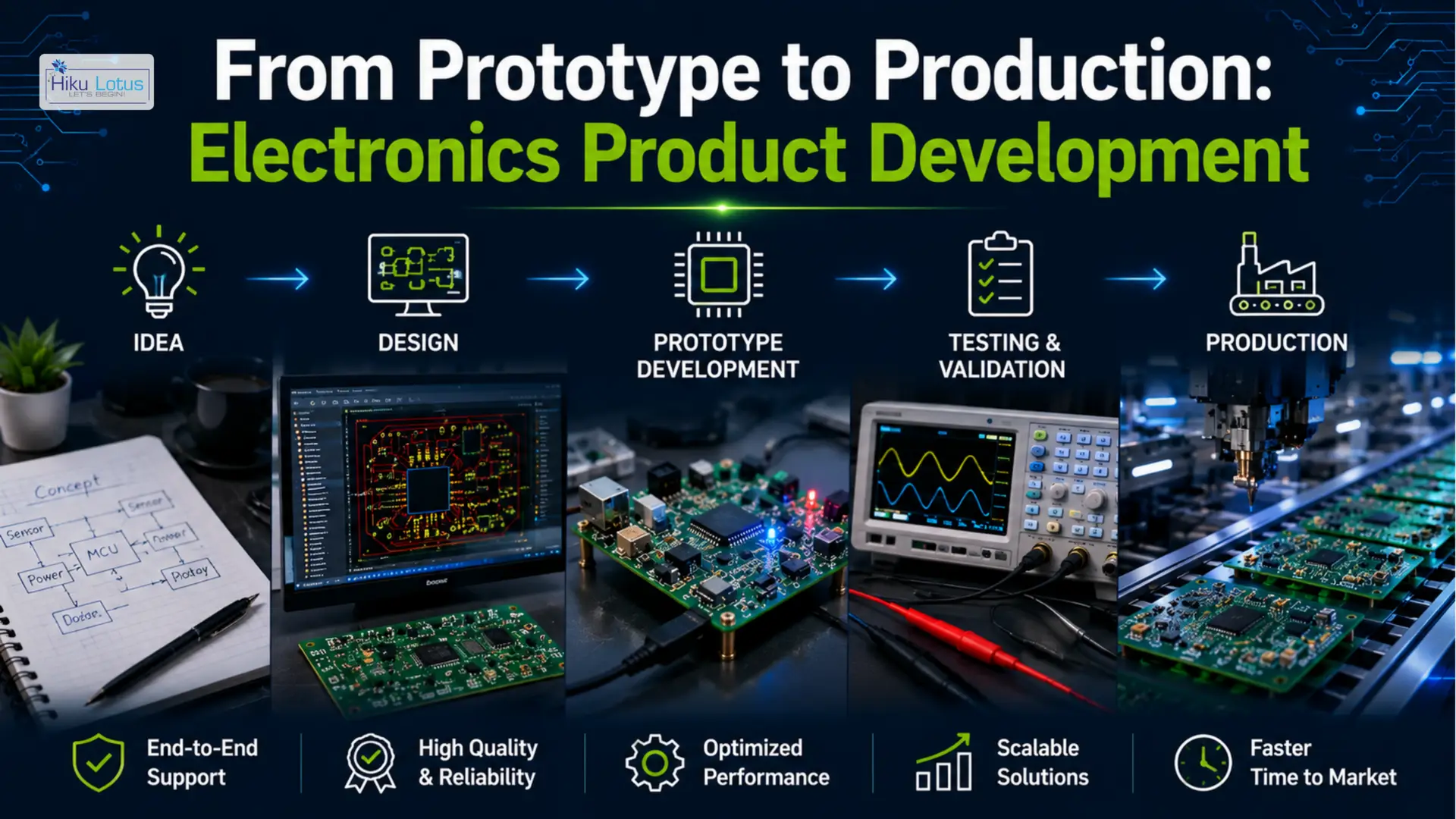
Idea → Requirements → Feasibility → Circuit Design → Component Selection → Schematic → PCB Layout → Prototype → Testing → Optimization → Production
Each stage contributes to the reliability and success of the final product.
1. Understanding the Product Idea
The first step is understanding what the product needs to accomplish.
At this stage, we focus on the application rather than immediately selecting components.
We look at questions such as:
- What does the product need to do?
- Who will use it?
- What inputs are required?
- What outputs are required?
- What sensors are involved?
- Are motors or actuators required?
- What communication interfaces are needed?
- What is the power source?
- Where will the product operate?
- What are the size constraints?
- What production quantity is expected?
The objective is to convert a basic idea into a clear technical direction.
For example, an initial requirement may simply be:
“We need a controller that receives sensor inputs, controls motors, displays information, and communicates wirelessly.”
This can then be converted into detailed engineering requirements.
2. Requirements Analysis
Once the product concept is understood, the next step is to define the technical requirements.
Requirements may include:
Electrical Requirements
- Input voltage
- Output voltage
- Current requirements
- Power consumption
- Analog inputs
- Digital inputs and outputs
- Protection requirements
Processing Requirements
- Microcontroller or processor
- Processing speed
- Memory
- Real-time requirements
- Data storage
Communication Requirements
- UART
- RS-232
- RS-485
- CAN
- SPI
- I²C
- Ethernet
- Wi-Fi
- Bluetooth / BLE
- RF
Environmental Requirements
- Operating temperature
- Humidity
- Vibration
- Dust
- Outdoor or indoor operation
Mechanical Requirements
- PCB dimensions
- Mounting holes
- Connector locations
- Enclosure constraints
- Height restrictions
Defining these requirements early creates a foundation for the rest of the development process.
3. Technical Feasibility Study
Before investing heavily in hardware development, the proposed solution should be technically evaluated.
A feasibility assessment can identify:
- Suitable controller architecture
- Required components
- Available technologies
- Power requirements
- Communication options
- Expected performance
- Potential technical risks
- Component availability
- Approximate development complexity
For example, if a product requires multiple motors, wireless communication, displays, sensors, and real-time control, the engineering team needs to determine whether a single microcontroller can handle all functions or whether a distributed architecture is more appropriate.
Early feasibility analysis can prevent expensive redesigns later.
4. System Architecture Development
Once the requirements are understood, the overall electronics architecture can be defined.
A typical architecture may look like:
Power Supply
↓
Protection & Power Management
↓
Main Microcontroller
↓
Sensors / Inputs / Communication
↓
Control Logic
↓
Drivers / Outputs / Actuators
Additional modules may include:
- Display controller
- Motor driver
- Wireless module
- Audio module
- Memory
- Communication interface
- Safety circuits
System architecture defines how these blocks communicate and interact with each other.
5. Component Selection
Selecting the right electronic components is one of the most important stages of development.
The cheapest component is not always the best component.
Selection should consider:
- Electrical specifications
- Availability
- Lifecycle
- Operating temperature
- Package type
- Reliability
- Power consumption
- Performance
- Cost
- Supplier availability
- Second-source possibilities
For microcontroller-based products, the MCU selection should consider:
- Number of GPIOs
- ADC channels
- Timers
- PWM channels
- Communication interfaces
- Flash memory
- RAM
- Processing performance
- Development ecosystem
Component selection should also consider the transition from prototype to production.
A component that is readily available for a prototype may not necessarily be the best long-term production choice.
6. Circuit and Schematic Design
After defining the architecture and selecting components, the detailed circuit design begins.
The schematic describes how all electronic components are electrically connected.
The design may include:
Power Supply
- Voltage regulators
- DC-DC converters
- Filters
- Protection circuits
Microcontroller Section
- MCU
- Clock
- Reset
- Programming interface
- Decoupling capacitors
Input Section
- Sensors
- Switches
- Buttons
- Analog inputs
Output Section
- LEDs
- Displays
- Relays
- MOSFETs
- Motor drivers
Communication Section
- UART
- RS-485
- CAN
- Ethernet
- Wireless modules
The schematic is reviewed for electrical correctness before moving to PCB layout.
7. PCB Stack-Up and Layer Planning
The next stage is determining the appropriate PCB structure.
Depending on the application, the board may use:
- 1-layer PCB
- 2-layer PCB
- 4-layer PCB
- 6-layer PCB
- Higher-layer-count PCB
Layer selection depends on factors such as:
- Circuit complexity
- Signal speed
- Power distribution
- EMI requirements
- Routing density
- Board size
- Manufacturing cost
For higher-performance electronics, additional layers can provide dedicated power and ground planes and improve signal integrity.
8. PCB Layout Design
The schematic now becomes a physical PCB.
PCB layout involves placing components and routing electrical connections while maintaining electrical, thermal, mechanical, and manufacturing requirements.
Important considerations include:
Component Placement
Components should be positioned according to:
- Signal flow
- Power requirements
- Thermal considerations
- Mechanical constraints
- Serviceability
Power Routing
High-current paths should be designed with suitable trace widths, copper thickness, and current-carrying capability.
Grounding
Proper ground-plane design helps reduce noise and provides controlled return paths.
High-Speed Signals
High-speed interfaces require careful routing to maintain signal integrity and reduce unwanted interference.
Analog and Digital Circuits
Sensitive analog sections may need to be separated from noisy digital or switching circuits.
Thermal Design
Heat-generating components should have adequate copper area, thermal vias, and appropriate airflow or heatsinking where required.
9. Design for EMI and EMC
Electromagnetic interference can cause serious problems in electronic products.
A PCB may work correctly on the workbench but experience unexpected behavior in a real operating environment.
EMI/EMC considerations can include:
- Ground-plane design
- Decoupling
- Filtering
- Signal routing
- Shielding
- Connector placement
- Switching-node control
- Cable routing
- Protection circuits
Considering EMI and EMC during PCB design is generally much more effective than attempting to fix interference problems after manufacturing.
10. Design for Manufacturing
A PCB should be designed not only to work electrically but also to be manufactured consistently.
Design for Manufacturing (DFM) considerations include:
- Component package selection
- PCB fabrication rules
- Track and spacing requirements
- Via sizes
- Soldering requirements
- Component orientation
- Assembly accessibility
- Automated assembly compatibility
The objective is to create a design that can move efficiently from engineering prototype to repeatable production.
11. Design for Testing
Testing should be considered during PCB development rather than added after the board is manufactured.
A production-friendly PCB may include:
- Test points
- Programming connectors
- Debug interfaces
- Status indicators
- Measurement points
- Diagnostic interfaces
These features can make troubleshooting and production testing significantly easier.
For products manufactured in higher quantities, automated or semi-automated testing can also be considered.
12. Prototype PCB Development
Once the PCB design is complete, prototype boards can be manufactured and assembled.
The prototype provides an opportunity to verify:
- Electrical functionality
- Mechanical fit
- Power consumption
- Communication
- Sensor operation
- Firmware interaction
- Thermal performance
- User interface
- System behavior
A prototype is not simply a demonstration board. It is an important engineering validation stage.
13. PCB Bring-Up and Debugging
When the prototype arrives, the first step is controlled board bring-up.
Typical checks include:
- Visual inspection
- Power supply verification
- Short-circuit checks
- Voltage measurements
- Clock verification
- MCU programming
- Communication testing
- Peripheral testing
- Input/output validation
- Functional testing
If a problem occurs, engineers may need to investigate the schematic, PCB layout, component selection, firmware, or external hardware.
Hardware and firmware debugging often need to happen together.
14. Firmware and Hardware Integration
For embedded products, PCB development and firmware development are closely connected.
The firmware may control:
- Sensors
- Motors
- Displays
- LEDs
- Relays
- Communication interfaces
- User inputs
- Safety functions
- Data logging
During prototype testing, hardware and firmware can be refined together to achieve the required system performance.
This hardware-firmware integration is particularly important for products based on microcontrollers and embedded processors.
15. Testing and Validation
Once the prototype is functional, comprehensive testing can begin.
Testing may include:
Functional Testing
Does every feature operate as intended?
Electrical Testing
Are voltages, currents, and signals within the required ranges?
Thermal Testing
Does the product remain within acceptable operating temperatures?
Communication Testing
Do all communication interfaces work reliably?
Stress Testing
Does the system remain stable under demanding operating conditions?
Environmental Testing
Where applicable, the product may be evaluated under temperature, humidity, vibration, or other environmental conditions.
Testing requirements depend on the product and its target market.
16. Design Optimization
Prototype testing often reveals opportunities for improvement.
The design may need optimization for:
- PCB size
- Cost
- Power consumption
- Thermal performance
- EMI
- Component availability
- Manufacturing
- Reliability
- Assembly
- Serviceability
For example, a prototype may function correctly but use too many components or have unnecessary wiring.
The engineering team can refine the design before production.
17. Preparing the PCB for Production
Once the design has been validated, the product can move toward production.
Production preparation may include:
- Final schematic
- Final PCB layout
- Gerber files
- Drill files
- Bill of Materials
- Pick-and-place files
- Assembly drawings
- Test procedures
- Programming procedures
- Firmware release
- Manufacturing documentation
This stage creates the documentation required for consistent production.
Prototype to Production: Why the Transition Matters
A prototype that works successfully does not automatically mean that the design is ready for mass production.
Production introduces additional considerations such as:
- Component availability
- Assembly yield
- Production testing
- Supply-chain risk
- Manufacturing cost
- Quality control
- Serviceability
- Regulatory requirements
A production-ready PCB should be designed with these factors in mind from the beginning.
Common Challenges in Electronics Development
Unclear Requirements
Incomplete requirements can lead to repeated design changes.
Solution: Define functional, electrical, mechanical, environmental, and production requirements early.
Component Availability
A selected component may become difficult to source.
Solution: Consider lifecycle, availability, and alternative components during design.
PCB Noise
Poor grounding and routing can cause unstable system behavior.
Solution: Apply proper grounding, decoupling, power distribution, and signal-routing practices.
Thermal Problems
Power components may generate more heat than expected.
Solution: Perform thermal analysis and provide appropriate copper area, thermal vias, heatsinks, or airflow.
Prototype-Only Thinking
A design may work as a prototype but become difficult or expensive to manufacture.
Solution: Apply DFM and DFT principles from the early design stages.
Our Electronics Development Approach at Hiku Lotus
At Hiku Lotus, we approach electronics development as an integrated engineering process rather than treating PCB design as an isolated activity.
Our capabilities include:
- Product requirement analysis
- Electronics feasibility studies
- System architecture
- Circuit design
- Component selection
- Schematic development
- PCB layout
- Multilayer PCB design
- Embedded hardware development
- Firmware development
- Sensor integration
- Communication interfaces
- Power electronics
- Motor and actuator control
- Prototype development
- Hardware-firmware integration
- Testing and debugging
- Design optimization
- DFM and DFT support
- Production support
This allows us to support projects from an early concept through prototype development and toward production.
Industries We Support
Our electronics development capabilities can be applied across a wide range of industries, including:
- Industrial automation
- Amusement and gaming
- IoT and IIoT
- Consumer electronics
- Embedded systems
- Control systems
- Automotive electronics
- Energy and power electronics
- Instrumentation
- Smart devices
- Specialized industrial equipment
Each industry has different technical requirements, but the fundamental electronics development process remains focused on functionality, reliability, manufacturability, and scalability.
From Idea to PCB: A Complete Development Journey
The complete process can be summarized as:
1. Idea
Define the product concept.
2. Requirements
Convert the concept into technical specifications.
3. Feasibility
Evaluate technology, components, risks, and architecture.
4. System Architecture
Define functional blocks and their relationships.
5. Component Selection
Choose suitable and production-ready components.
6. Circuit Design
Develop and review the schematic.
7. PCB Design
Create the board layout and routing.
8. Prototype
Manufacture and assemble the first PCB.
9. Bring-Up
Power, program, debug, and verify the board.
10. Testing
Validate electrical and functional performance.
11. Optimization
Improve reliability, cost, performance, and manufacturability.
12. Production
Prepare the validated design for manufacturing.
This structured approach helps transform an initial electronics idea into a practical and dependable product.
Conclusion
Turning an electronics idea into a working PCB requires careful engineering at every stage. The process involves much more than drawing a schematic and routing a board. Requirements, component selection, circuit architecture, PCB layout, firmware, testing, manufacturing, and long-term reliability all need to be considered.
A structured electronics development process helps reduce design risks, minimize costly redesigns, improve product reliability, and create a smoother transition from prototype to production.
At Hiku Lotus, we combine electronics engineering, PCB design, embedded systems, firmware development, prototyping, testing, and production support to help businesses turn ideas into real electronic products.
Talk to Hiku Lotus About Your Electronics Product Development Project
Have an electronics idea, circuit concept, prototype, or existing design that needs to become a reliable PCB? Hiku Lotus provides complete electronics development support, from requirements analysis and circuit design to PCB layout, embedded firmware, prototyping, testing, optimization, and production support. Get in touch with our team to discuss your requirements and take your electronics idea from concept to a production-ready solution.
Frequently Asked Questions
1. Can Hiku Lotus develop a PCB from an initial product idea?
Yes. Hiku Lotus can help convert an initial product concept into technical requirements, system architecture, circuit design, PCB layout, prototype development, and testing.
2. What information is required to start an electronics development project?
The available information may include product functionality, inputs and outputs, power requirements, sensors, communication requirements, mechanical constraints, operating environment, and expected production volume.
3. Does Hiku Lotus provide PCB design services?
Yes. PCB development can include schematic design, component selection, PCB layout, multilayer PCB design, DFM, DFT, and manufacturing documentation.
4. Can you develop the firmware along with the PCB?
Yes. Embedded firmware can be developed alongside the hardware to provide hardware-firmware integration and system-level functionality.
5. Can an existing PCB be redesigned or improved?
Yes. Existing electronics can be analyzed and redesigned to address performance issues, obsolete components, cost, reliability, functionality, or manufacturing requirements.
6. Do you support prototype development?
Yes. Prototype development and testing can be included as part of the electronics development process.
7. Can a prototype PCB be prepared for mass production?
Yes. After prototype validation, the design can be optimized for manufacturing, component availability, testing, assembly, cost, and production requirements.
8. How early should manufacturing considerations be included?
Manufacturing considerations should ideally be included from the early design stages. Applying DFM and DFT principles early can reduce redesigns and production problems later.